-
PRODUCTS
- HV GaN HEMT
- LV GaN HEMT
- Design Support
- Gate Drivers/Controllers
- Management of Hazardous Substances
- Work With Us
-
APPLICATIONS
-
TECHNOLOGY
-
Quality & Reliability
- Quality Policy
- Quality System
- Qualification Summary
- Reliability Report
- Reliability Stress Model
- Ongoing Reliability Monitoring
- Reliability Testing Facilities
- Failure Analysis Laboratory
- Certifications
- WHERE TO BUY
-
ABOUT US
- Company
- Citizenship
- EHS Management
- Partners
- Investors
- News & Events
- Career
- Suzhou Fab video
- Zhuhai Fab video
Consumer
-

Description
Today, our mobile phone are getting more and more powerful and there is a need to charge them faster and faster. Therefore, the power delivery (PD) chargers technology is evolving towards higher efficiency and higher power density, which allows adapters to be more powerful, and thus charge our phone faster, without increasing their size and wasting energy as heat. In order to achieve such objective, the adapter system needs to be more efficient and needs to operate at higher frequency that allow to use smaller passive components. The high frequency and high efficiency characteristics of Innoscience’s GaN technology meet these requirements enabling efficient and compact adapters. Several adapters (in-box and out-box) are already successfully using Innoscience’s GaN technology and sold in the consumer market.
Compared with traditional Si MOSFET, GaN has the following advantages:
1 Low Qg/Ciss: faster turn-on and turn-off, higher switching speed, reduce switching losses.
2 Low Coss/Qoss: faster turn-on and turn-off and higher switching frequency, reduce switching losses.
3 Qrr=0: No reverse recovery losses (absence of body diode), Reduce switching noise, better EMI performance.
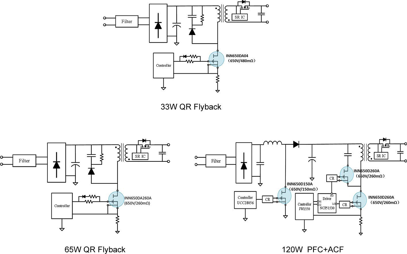
4 Low RDSON: reduce conduction losses.Solution topology view Main parameters of the scheme
Scheme 1:SMPS——33W QR Flyback Topology QR Flyback Input voltage 90-264Vac Output 3.3V~20V,11V/3A(max) Frequency 120KHz@230Vac Transformer ATQ1715,JPP95 Efficiency 92.9% @230Vac & 20V/1.5A Size 26*26*26mm(PCBA) Watt density 30.8W/in3 Device INN650DA04 Control IC JW1515H+JW7726B Scheme 2:SMPS——65W QR Flyback Topology QR flyback Input voltage 90-264Vac Output 20V/3.25A Frequency 135kHz @230Vac Transformer ATQ23.7,JPP95 Efficiency 94.1% @230Vac & 20V/3.25A Size 48.7*27*26mm(PCBA) Watt density 31W/in3(PCBA) Device INN650DA260A Control IC NCP1342+MP6908A Scheme 3:SMPS——120W PFC+ACF Topology Boost PFC+ACF Input voltage 90-264Vac Output 120W max ACF Frequency 230kHz @120W Transformer ATQ23,NVM02 Efficiency 94.5% @230Vac & 20V/6A Size 46*46*26mm(PCBA) Watt density 35.7W/in3(PCBA) Device INN650D150A+INN650D260A*2 Control IC NCP1622+JW1550 -

Wireless Charging
Compared to traditional Silicon technology, Innoscience’s GaN technology has the advantages of smaller parasitic capacitance, faster switching speed and smaller on-resistance per unit area. When applied to wireless charging system, Innoscience’s GaN technology reduces both the switching and conduction loss, thus enabling wireless charging system with higher system efficiency and longer transmission distance.
Solution topology view
-

Class-D Audio Amplifier
The power loss of Class-D amplifier is much smaller than classical linear amplifier thanks to the fact that the Class-D amplifier operates in switching mode. This bring several benefits, which are among others: better sound quality, less heat, higher efficiency, smaller circuit board and thus smaller audio system, lower cost, extending battery life in portable systems etc… InnoGaNTM transistors area ideal for class-D amplifier by combining fast switching speed, low switching loss, small parasitic capacitance etc..
The power transistor in Class-D amplifier operates in switching mode and generate a train of voltage pulses output. Thus, a low-pass filter is often inserted between the output stage and the speaker. Since most audio signals are not pulse trains, a modulator must be included in a Class-D amplifier to convert the audio input into pulses, so the pulses can drive the power transistor to operate. Since the Class-D amplifier operate in switching mode, the switching loss of the transistors become key for the system performance, which is why GaN technology is often used in Class-D amplifier for audio system. Compared to traditional Silicon transistors, InnoGaNTM transistors show: faster switching speed, lower switching loss, smaller parasitic capacitance (Coss) lower energy stored in output capacitance (Eoss), No reverse recovery losses (Qrr=0 thanks to the absence of the body diode). Moreover, lower switching loss enables to increase the pulse width modulation (PWM) frequency, which allow to reduce the size (and loss) of the low-pass filters. Furthermore, since Innoscience’s GaN (InnoGaNTM) devices switch fast, it is recommend to reduce the dead time of the PWM.
Solution topology view
-

Over Voltage Protection (OVP)
The Over Voltage Protection (OVP) unit function is to protect the main system by shutting down the unit when the input voltage exceeds a defined value. The size of each unit inside a mobile phone or laptop is of paramount importance and InnoGaNTM transistors enable the OVP unit to be 50% smaller than the one made with Silicon technology. This is achieved by replacing two MOSFET devices with one InnoGaNTM bi-directional transistor. Indeed, thanks to the absence of the body diode, InnoGaNTM realizes the bidirectional shutdown on its own. At the same time, the overall system losses are reduced thanks to the lower on-resistance of InnoGaNTM devices compared to Silicon MOSFET. This increases the charging efficiency and produce less heat.
Solution topology view Main parameters of the scheme
Bi-GaN Part Number INN40W08 Configuration Single VDD(Max)/V 40 ID( continous current , max)/A 15 RDD(on)(type)/mOhm 5.5 Package(mm) 2X2 -

Time-of-flight (ToF)
The resolution and measure distance in LIDAR systems based on Time-of-flight (ToF) is determined by the laser driver of the system. InnoGaNTM transistors are today used in ToF applications to drive the laser as they provide simultaneously higher current (i.e. longer measure distance) and narrower pulse width (i.e. higher resolution) compared to traditional Silicon technology. Therefore, Innoscience’s GaN Technology with smaller area cost and higher performance is a better choice for ToF system.
Solution topology view.png)

 English
 中文
中文
